
Our Quick-Turn PCB Prototype Orders
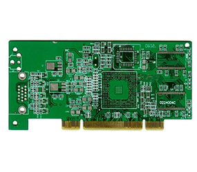
Data Acquisition Motherboard
2L
TG170
2OZ
HDI PCB
2-N-2
Order Size: 0.2㎡
Quickest Time: 5 days
16-layer HDI blind buried hole semiconductor test board
16L
6MM
HDI
From $5/10pcsBuild
Time:24 hours
Data Acquisition Motherboard
16L
6MM
HDI
From $5/10pcsBuild
Time:24 hours

Thick copper high level board
16L
6MM
HDI
From $5/10pcsBuild
Time:24 hours
4+2 rigid-soft boards
16L
6MM
HDI
From $5/10pcsBuild
Time:24 hours
Thick copper high level board
16L
6MM
HDI
From $5/10pcsBuild
Time:24 hours
16-layer HDI blind buried hole semiconductor test board
16L
6MM
HDI
From $5/10pcsBuild
Time:24 hours
4+2 rigid-soft boards
16L
6MM
HDI
From $5/10pcsBuild
Time:24 hours
Affordable Prototype PcB Manufacturer in China
Latest order
Today's new order: 1292 
Date
Buyer Name
Layers
Size
Lead Time
-
07-22
 Tom Json
610*10cm4-5 days
Tom Json
610*10cm4-5 days -
07-21
 Lily kitty
1210*30cm2-3 days
Lily kitty
1210*30cm2-3 days -
07-02
 Bright
820*10cm1-2 days
Bright
820*10cm1-2 days -
07-06
 Jordan
420*20cm1-2 days
Jordan
420*20cm1-2 days -
06-28
 Jack
1020*30cm1-2 days
Jack
1020*30cm1-2 days -
07-03
 Michael
1630*10cm1-2 days
Michael
1630*10cm1-2 days -
06-20
 Tony
1040*20cm1-2 days
Tony
1040*20cm1-2 days -
06-18
Steve
1230*10cm1-2 days
-
07-26
alexia
820*10cm1-2 days
-
06-26
amelia
1210*10cm1-2 days
-
06-23
Michael
1440*20cm1-2 days
-
06-24
alexia
1210*20cm1-2 days
-
06-25
Michael
820*20cm2-3 days
-
07-6
Tony
430*20cm1-2 days
-
07-15
Jordan
220*20cm4-5 days
-
07-16
Steve
810*20cm1-3 days
-
07-20
Tom Json
610*20cm2-4 days
-
08-16
alexia
520*30cm3-4 days
-
08-06
Tom Json
1050*20cm1-4 days
-
08-12
Michael
610*20cm2-3 days
-
08-13
alexia
810*20cm3-4 days
-
08-06
amelia
610*30cm2-5 days
-
08-07
Lily kitty
410*50cm1-3 days
-
08-08
Jack
320*20cm2-4 days
SALE
Instant Quote
Full feature prototype PCB custom service at low cost.
Dimensions
x
mm
Quantity
Layers
Thickness
Get $5.00 - Free Prototype Order
Why JH-PCBA can so quickly?

Fast quote
by sales: Our engineers have more than 10-year experiences in PCB field, can review your gerber file professionally and fast.
10min for 1-4L
2h for 12-18L
30 min for 6-10L
1d for 18-28L
complex boards and big quantity boards inquires , latest next day
Online quote and order placed by yourself.

Professional and powerful Engineers team to deal with EQ and WF
50 engineers, over 10 years experience in PCB industry, familiar with PCB industry standards and customers’ requests
EQ and WF(working file) feedback with 12h;
6*24h engineering service

Quality Assurance
120 QA&QC
Full testing equipment, such as Metallurgical microscope, Impedance tester, AOI, X-RAY Thickness Test…
100% passes full test. Professional test report can be provided if you need.

Quick Turn Lead Time
2L PCB in 24h fastest, 4-6L PCB in 48h;
6/8L PCB in 72h, 10L PCB in 96h;
We promise:
Expedite order on time delivery rate reaches 99%. Should any delay occur, we will return all the expedite fees and offer discount so that you can better maintain the customers.
Fast proofing lead time table
| Layers | PCB Order Size (m2) |
Normal Lead Time (wds) |
Quickest Lead Time (Hours) |
|---|---|---|---|
| 2 Layers | < 1 m2 | 5 | 8 |
| 1-5 m2 | 8 | 24 | |
| 5-10 m2 | 10 | 24 | |
| 10-30 m2 | 12 | 24 | |
| 30-50 m2 | 14 | 48 | |
| 4 Layers | < 1 m2 | 6 | 24 |
| 1-5 m2 | 9 | 48 | |
| 5-10 m2 | 11 | 72 | |
| 10-30 m2 | 13 | 72 | |
| 30-50 m2 | 15 | 96 | |
| 6/8 Layers | < 1 m2 | 7 | 24 |
| 1-5 m2 | 10 | 48 | |
| 5-10 m2 | 12 | 72 | |
| 10-30 m2 | 14 | 72 | |
| 30-50 m2 | 16 | 96 | |
| 10 Layers | < 1 m2 | 9 | 72 |
| 1-5 m2 | 11 | 96 | |
| 5-10 m2 | 13 | 96 | |
| 10-30 m2 | 15 | 120 | |
| 30-50 m2 | 17 | 120 | |
| 10 or more Layers | < 1 m2 | 9 | 72 |
| 1-5 m2 | 11 | 96 | |
| 5-10 m2 | 13 | 96 | |
| 10-30 m2 | 15 | 120 | |
| 30-50 m2 | 17 | 120 |
Advanced High-quality PCB Manufacturing Capabilities
| No. | Item | Process capability parameter | |
|---|---|---|---|
| 1 | Base material | FR-4|High Tg|Halogen-free|PTFE|Ceramic PCB (Scrap rate is too high)|Polyimide | |
| 2 | PCB type | PCB|FPC|R-FPC|HDI | |
| 3 | Max layer count | 64 layers | |
| 4 | Min base copper thickness | 1/3 OZ (12um) | |
| 5 | Max finished copper thickness | 8 OZ | |
| 6 | Min trace width/spacing | Inner layer | 2/2mil (H/H OZ base copper)only part trace with this width and space but not all the board with this trace width and space |
| 7 | Outer layer | 2/2mil (1/3 OZ base copper)only part trace with this width and space but not all the board with this trace width and space | |
| 8 | Min spacing between hole to inner layer conductor | 6mil | |
| 9 | Min spacing between hole to outer layer conductor | 6mil | |
| 10 | Min annular ring for via | 3mil | |
| 11 | Min annular ring for component hole | 5mil | |
| 12 | Min BGA diameter | 8mil | |
| 13 | Min BGA pitch | 0.4mm | |
| 14 | Min hole size | 0.15mm(CNC)|0.1mm(Laser Blind/buried vias) | |
| 15 | Max aspect ratios | 20:1 | |
| 16 | Min soldermask bridge width | 3mil | |
| 17 | Soldermask/circuit processing method | Film|LDI | |
| 18 | Min thickness for insulating layer | 2mil | |
| 19 | HDI & special type PCB | HDI(1-7 steps)|R-FPC(2-16 layers)|High frequency mix-pressing(2-20 layers)|Buried capacitance & resistance …… | |
| 20 | Surface Finish type | ENIG|HAL|HAL lead free|OSP|Immersion Sn|Immersion silver|Plating hard gold|Plating silver | |
| 21 | Max PCB size | 609*889mm | |
